Tag Archives: 6nm

Sony PlayStation 5 consoles now ship with smaller 6nm AMD SoC called “Oberon Plus”

PlayStation 5 gets 6nm SoC

According to Angstronomics, a third model of PS5 console codenamed “CFI-1202” comes with a smaller SoC called “Oberon Plus”. 

The latest variant of the Sony console features an updated SoC manufactured using TSMC 6nm process technology. This smaller node is compatible with 7nm node that has been used for Sony PS5 “Oberon” SoC until now.

The 6nm port of Oberon has the same design and introduces no changes to the processor configuration. That said, the underlying Zen2 compute and RDNA2 graphics architectures have not changed.

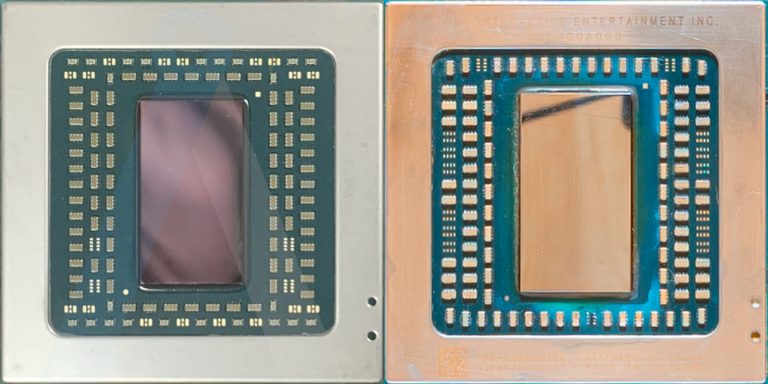
Oberon Plus SoC (left) vs Oberon (right), Source: Angstronomics

The discovery of the new SoC comes weeks after first reports of the new console variant that has been spotted in Australia. As it turns out, the new version not only has upgraded internals, such as a new mainboard, smaller and lighter cooler, but also an updated silicon powering the console. A full teardown of the 3rd variant of PS5 console has been posted by Austin Evans earlier this month.

[Austin Evans] The new PS5 is BETTER 😬 (949,339 views)

The design and specifications of Oberon Plus are identical to the 7nm variant, however the chip is smaller, around 260 mm² compared to the original 300 mm². These changes mean that the console requires less power and less demanding cooling solution.

For AMD and Sony, this also means that more chips can be made with one wafer, so the estimated production cost of the updated console could be up to 12% lower. Microsoft Xbox Series, which are also based on 7nm AMD SoC, are to be updated with 6nm designs in the future as well.

Source: Angstronomics


Read original article here

Sony’s Updated PS5 Console Comes With 6nm AMD Oberon Plus SOC, Offers Lower Temps & Consumes Lower Power

Sony recently did a soft refresh of its PS5 console with a new variant known as the CFI-1202 that offers lower temps & power input. The new console is lighter, runs cooler, and consumes lower power & this is all thanks to the refreshed AMD Obreon Plus SOC hailing the TSMC 6nm process node.

Sony’s PS5 “CFI-1202” Console Variant Features Enhanced 6nm AMD Oberon Plus SOC: Reduced Die Size, Lower Power & Cooler Operation

In a recent teardown video published by Austin Evans, the Techtuber noticed that the Sony PS5 console was shipping in a new variant that is lighter, cooler, & less power hungry. This new PS5 variant is labeled as the “CFI-1202” and we can now get to the bottom of why it is so better than Sony’s original PS5 variants (CFI-1000 / CFI-1001).

Tech outlet, Angstronomics, has confirmed in their exclusive that the Sony PS5 (CFI-1202) comes with an enhanced AMD Oberon SOC known as Oberon Plus which utilizes the TSMC N6 process (6nm). TSMC has made it so that their 7nm (N7) process node is design rule compatible with the 6nm EUV (N6) node. This allows TSMC partners to easily port existing 7nm chips to the 6nm node without running into major complexities. The N6 process node offers an 18.8% transistor density increase and also reduces power consumption which in return reduces temperatures.

AMD’s 6nm Oberon Plus SOC for Sony’s refreshed PS5 console is 15% smaller than the 7nm Oberon SOC (Image Credits: Angstronomics)

This is why the new Sony PS5 consoles are lighter and feature a smaller heatsink compared to the launch variants. But that’s not all, we also get to see a brand new chip shot of the AMD Oberon Plus SOC sitting next to the 7nm Oberon SOC. The new die measures around 260mm2 which is a 15% reduction in die size compared to the 7nm Oberon SOC (~300mm2). There’s another advantage of moving to 6nm and that’s the number of chips that can be produced on a single wafer. The outlet reports that each Oberon Plus SOC wafer can produce around 20% more chips at the same cost.

What this means is that without affecting their cost, Sony can offer more Oberon Plus chips to be used in PS5 and that can further reduce shortages in the market that the current-gen consoles have faced since their launch. It is also reported that TSMC will phase out 7nm Oberon SOCs in the future and move entirely to 6nm Oberon Plus SOC which will result in 50% more chips to be made per wafer. Microsoft is also expected to utilize the 6nm process node for its refreshed Arden SOC in the future for its Xbox Series X consoles.

News Source: Angstronomics

Products mentioned in this post


Read original article here

8 Enhanced 6nm Zen 3 Cores, 20 MB Cache, 4.6 GHz Boost & Radeon 680M ‘RDNA 2’ Integrated Graphics

Today we have an interesting leak for those who are waiting for next-gen AMD laptops powered by the Rembrandt Ryzen 6000 APU such as the Ryzen 9 6900HX.

AMD High-Performance Laptops With Ryzen 9 6900HX ‘Rembrandt’ APU To Pack 8 Enhanced Zen 3 Cores on 6nm Process & Radeon 680M ‘RDNA 2’ iGPU

Our sources have told us quite a few details regarding the AMD Rembrandt APUs, especially the Ryzen 9 6900HX, which is going to be one of the fastest Ryzen 6000 chips in the pack. AMD’s new APU lineup will be replacing the Ryzen 5000 ‘Cezanne’ series and feature an update to both CPU and GPU IPs.

AMD Navi 24 ‘RDNA 2’ To Be The First 6nm GPU, Will Power Entry-Level Radeon RX 6500 XT & RX 6400 Graphics Cards

On the CPU side, AMD’s Ryzen 9 6900HX APU is going to offer 8 cores and 16 threads. These cores are based on the new Zen 3+ architecture which is an enhanced version of the Zen 3 core but with the latest TSMC 6nm alternation. The new process node would allow AMD to squeeze more juice out of its laptop chips while running efficiently. As for cache, the chip will come with 16 MB of L3 & 4 MB of L2 cache. For those expecting 3D V-Cache technology on laptops, that isn’t happening till a few more generations.

Coming to the clock speeds, the max boost clock for the chip is going to be rated at 4.6 GHz which is the same as the current Ryzen 9 5900HX but we can expect the Ryzen 9 6900HX to draw lesser power. The CPU will allow for DDR5-4800 memory support on laptops which will deliver a massive increase in bandwidth over DDR4 memory.

The GPU side for the AMD Rembrandt Ryzen 9 6900HX is going to see a major upgrade. AMD will be utilizing its RDNA 2 core architecture and while we weren’t told how many RDNA 2 CUs we will be getting on the new chips, we are told that team red has decided to change the nomenclature of its integrated RDNA graphics. Starting with Rembrandt, AMD will use the Radeon 6**M branding. The particular iGPU variant for the Ryzen 9 6900HX will be called Radeon 680M. The DDR5 addition plays a crucial role for the integrated graphics as RDNA 2 loves raw bandwidth and the extra juice from the new memory standard is definitely going to help here.

But since the AMD Ryzen 9 6900HX is going to be targeted at high-performance notebooks, we are told that most designs that this APU will be featured inside will be fitted with NVIDIA’s top GeForce GPUs such as the RTX 3070 Ti (8 GB) and RTX 3080 Ti (16 GB). We have already seen some designs from ASUS leak out earlier including their ROG Zephyrus and ROG STRIX. Expect more information from AMD at the CES 2022 virtual keynote.

AMD Ryzen 9 6900HX ‘Rembrandt’ APU Specs

APU Name AMD Ryzen 9 6900HX AMD Ryzen 9 5900HX AMD Ryzen 9 4900H
Core Architecture Zen 3+ Zen 3 Zen 2
Process Node 6nm 7nm 7nm
Cores / Threads 8 / 16 8 / 16 8 / 16
Max Clocks 4.6 GHz 4.6 GHz 4.4 GHz
Cache (L3+L2) 20 MB 20 MB 12 MB
Memory Support DDR5-4800
LPDDR5X?
DDR4-3200
LPDDR4-4266
DDR4-3200
LPDDR4-4266
Graphics Architecture RDNA 2 Vega++ Vega+
Graphics Codename Radeon 680M Radeon Vega 8 Radeon Vega 8
Graphics Compute Units TBC 8 8
TDP 35-54W? 35-54W 35-54W
Launch Q1 2022 Q1 2021 Q1 2020


Read original article here

AMD Unveils Instinct MI200 ‘Aldebaran’ GPU, First 6nm MCM Product With 58 Billion Transistors, Over 14,000 Cores & 128 GB HBM2e Memory

AMD has officially announced its next-generation MI200 HPC GPU codenamed Aldebaran that uses a 6nm CDNA 2 architecture to deliver insane compute performance.

AMD Unveils Instinct MI200, Powering The Next-Gen Compute Powerhouse With First 6nm MCM GPU Technology & Over 95 TFLOPs FP32 Performance

AMD is officially the first to MCM technology and they are doing so with a grand product which is their Instinct MI200 codenamed Aldebaran. The AMD Aldebaran GPU will come in various forms & sizes but it’s all based on the brand new CDNA 2 architecture which is the most refined variation of Vega. Some of the main features before we go into detail are listed below:

AMD Unveils Next-Gen EPYC Milan-X CPUs, First To Feature 3D V-Cache Tech With Insane 804 MB Cache

  • AMD CDNA 2 architecture – 2nd Gen Matrix Cores accelerating FP64 and FP32 matrix operations, delivering up to 4X the peak theoretical FP64 performance vs. AMD previous-gen GPUs.
  • Leadership Packaging Technology – Industry-first multi-die GPU design with 2.5D Elevated Fanout Bridge (EFB) technology delivers 1.8X more cores and 2.7X higher memory bandwidth vs. AMD previous-gen GPUs, offering the industry’s best aggregate peak theoretical memory bandwidth at 3.2 terabytes per second.
  • 3rd Gen AMD Infinity Fabric technology – Up to 8 Infinity Fabric links connect the AMD Instinct MI200 with 3rd Gen EPYC CPUs and other GPUs in the node to enable unified CPU/GPU memory coherency and maximize system throughput, allowing for an easier on-ramp for CPU codes to tap the power of accelerators.

AMD Instinct MI200 GPU Die Shot:

Inside the AMD Instinct MI200 is an Aldebaran GPU featuring two dies, a secondary and a primary. It has two dies with each consisting of 8 shader engines for a total of 16 SE’s. Each Shader Engine packs 16 CUs with full-rate FP64, packed FP32 & a 2nd Generation Matrix Engine for FP16 & BF16 operations.

Each die, as such, is composed of 128 compute units or 8192 stream processors. This rounds up to a total of 220 compute units or 14,080 stream processors for the entire chip. The Aldebaran GPU is also powered by a new XGMI interconnect. Each chiplet features a VCN 2.6 engine and the main IO controller.

Built on AMD CDNA 2 architecture, AMD Instinct MI200 series accelerators deliver leading application performance for a broad set of HPC workloads. The AMD Instinct MI250X accelerator provides up to 4.9X better performance than competitive accelerators for double precision (FP64) HPC applications and surpasses 380 teraflops of peak theoretical half-precision (FP16) for AI workloads to enable disruptive approaches in further accelerating data-driven research.

In terms of performance, AMD is touting various record wins in the HPC segment over NVIDIA’s A100 solution with up to 3x performance improvements in AMG.

Watch The AMD ‘Accelerated Data Center’ Premiere Live Event Here – Next-Gen EPYC & Instinct Announcements

As for DRAM, AMD has gone with an 8-channel interface consisting of 1024-bit interfaces for an 8192-bit wide bus interface. Each interface can support 2GB HBM2e DRAM modules. This should give us up to 16 GB of HBM2e memory capacity per stack and since there are eight stacks in total, the total amount of capacity would be a whopping 128 GB. That’s 48 GB more than the A100 which houses 80 GB HBM2e memory. The memory will clock in at an insane speed of 3.2 Gbps for a full-on bandwidth of 3.2 TB/s. This is a whole 1.2 TB/s more bandwidth than the A100 80 GB which has 2 TB/s.

The AMD Instinct MI200 will be powering three top-tier supercomputers which include the United States’ exascale Frontier system; the European Union’s pre-exascale LUMI system; and Australia’s petascale Setonix system. The competition includes the A100 80 GB which offers 19.5 TFLOPs of FP64, 156 TFLOPs of FP32 and 312 TFLOPs of FP16 compute power. But we are likely to hear about NVIDIA’s own Hopper MCM GPU next year so there’s going to be a heated competition between the two GPU juggernauts in 2022.

AMD Radeon Instinct Accelerators 2020

Accelerator Name AMD Instinct MI300 AMD Instinct MI250X AMD Instinct MI250 AMD Instinct MI100 AMD Radeon Instinct MI60 AMD Radeon Instinct MI50 AMD Radeon Instinct MI25 AMD Radeon Instinct MI8 AMD Radeon Instinct MI6
GPU Architecture TBA (CDNA 3) Aldebaran (CDNA 2) Aldebaran (CDNA 2) Arcturus (CDNA 1) Vega 20 Vega 20 Vega 10 Fiji XT Polaris 10
GPU Process Node Advanced Process Node Advanced Process Node Advanced Process Node 7nm FinFET 7nm FinFET 7nm FinFET 14nm FinFET 28nm 14nm FinFET
GPU Dies 4 (MCM)? 2 (MCM) 2 (MCM) 1 (Monolithic) 1 (Monolithic) 1 (Monolithic) 1 (Monolithic) 1 (Monolithic) 1 (Monolithic)
GPU Cores 28,160? 14,080 14,080? 7680 4096 3840 4096 4096 2304
GPU Clock Speed TBA 1700 MHz ~1700 MHz ~1500 MHz 1800 MHz 1725 MHz 1500 MHz 1000 MHz 1237 MHz
FP16 Compute TBA 383 TOPs TBA 185 TFLOPs 29.5 TFLOPs 26.5 TFLOPs 24.6 TFLOPs 8.2 TFLOPs 5.7 TFLOPs
FP32 Compute TBA 95.8 TFLOPs TBA 23.1 TFLOPs 14.7 TFLOPs 13.3 TFLOPs 12.3 TFLOPs 8.2 TFLOPs 5.7 TFLOPs
FP64 Compute TBA 47.9 TFLOPs TBA 11.5 TFLOPs 7.4 TFLOPs 6.6 TFLOPs 768 GFLOPs 512 GFLOPs 384 GFLOPs
VRAM TBA 128 GB HBM2e 128 GB HBM2e 32 GB HBM2 32 GB HBM2 16 GB HBM2 16 GB HBM2 4 GB HBM1 16 GB GDDR5
Memory Clock TBA TBA TBA 1200 MHz 1000 MHz 1000 MHz 945 MHz 500 MHz 1750 MHz
Memory Bus TBA 8192-bit 8192-bit 4096-bit bus 4096-bit bus 4096-bit bus 2048-bit bus 4096-bit bus 256-bit bus
Memory Bandwidth TBA ~2 TB/s? ~2 TB/s? 1.23 TB/s 1 TB/s 1 TB/s 484 GB/s 512 GB/s 224 GB/s
Form Factor TBA Dual Slot, Full Length / OAM Dual Slot, Full Length / OAM Dual Slot, Full Length Dual Slot, Full Length Dual Slot, Full Length Dual Slot, Full Length Dual Slot, Half Length Single Slot, Full Length
Cooling TBA Passive Cooling Passive Cooling Passive Cooling Passive Cooling Passive Cooling Passive Cooling Passive Cooling Passive Cooling
TDP TBA 500W TBA 300W 300W 300W 300W 175W 150W

The Aldebaran MI200 GPU will come in three configurations, the OAM only MI250 and MI250X & the dual-slot PCIe MI210. AMD has only shared full specifications and performance figures for its MI250 class HPC GPUs. The MI250X features the full 14,080 configurations and delivers 47.9, 95.7, 383 TFLOPs of FP64/FP32/FP16 while the MI250 features 13,312 cores with 45.3,90.5,362.1 TFLOPs of FP64/FP32/FP16 performance. The memory configuration remains the same between the two GPU configurations.

AMD Instinct MI200 GPU Package:


Read original article here